Development System Reference Guide

Preface
About This Manual
The Development System Reference Guide contains information on the software programs in the Xilinx Development System. Generally, the chapters are organized in the following way.
- A brief summary of program functions
- A syntax statement
- A review of the input files used and the output files generated by the program
- A listing of the commands, options, or parameters used by the program
- Examples of how you can use the program
For an overview of the Xilinx Development System describing how these programs are used in the design flow, see the Development System User Guide.
You must consult The Programmable Logic Data Book for device-specific information on Xilinx device characteristics, including readback, boundary scan, configuration, length count, and debugging. The Programmable Logic Data Book is available in hard copy and on the Xilinx web site (http://www.xilinx.com). See http://www.xilinx.com/partinfo/databook.htm for the current version of this book.
For specific design issues or problems, use the Answers Search function on the Web (http://www.xilinx.com/support/searchtd.htm) to access the following.
- Answers Database: current listing of solution records for the Xilinx software tools
- Applications Notes: descriptions of device-specific design techniques and approaches
- Data Sheets: pages from The Programmable Logic Data Book
- XCELL Journal: quarterly journals for Xilinx programmable logic users
- Expert Journals: the latest news, design tips, and patch information on the Xilinx design environment
If you cannot access the Web, you can install and access the Answers book with the DynaText online browser in the same manner as the Xilinx book collection. The Answers book includes information in the Answers Database at the time of this release.
The Design Flow
The following figure shows the three parts of the Xilinx design flow: design entry, design implementation, and design verification.
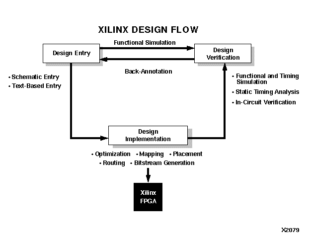
Design entry takes the design from concept to netlist. There are a number of ways to enter a design, including schematics, Boolean or state expressions, hardware description languages (HDLs) such as Verilog and VHDL, EDIF or XNF netlists from earlier designs, and cores. These entry methods require CAE tools to produce a design file in EDIF or XNF netlist format.
Design implementation starts by converting the netlist to Native Generic Database (NGD) format, and ultimately produces a configuration bitstream for the target FPGA device. It includes optimization and mapping, placement and routing, and bitstream creation. Designs can be implemented automatically or by using a combination of the automatic and manual Xilinx Development System tools.
Design verification includes simulation, static-timing analysis, and in-circuit verification. Simulation is performed using third-party tools which are supported by Xilinx. The input for these tools requires a tool-specific translation of an NGD file to a simulation netlist. You can simulate an NGD file at any point in the design flow. Static-timing analysis tools and in-circuit verification tools are part of the Xilinx Development System. Consult the “Design Implementation” chapter in the Development System User Guide for a more detailed description.
Manual Contents
The Development System Reference Guide provides detailed information about converting, implementing, and verifying designs in the Xilinx environment. Check the program chapters for information on what program works with each family of FPGA device. The following is a brief overview of the contents and organization of the Development System Reference Guide.
- Chapter 1, “Introduction,” - Describes some basics that are common to the different Xilinx Development System modules.
- Chapter 2, “NGDBuild,” - NGDBuild performs all of the steps necessary to read a netlist file in XNF or EDIF format and create an NGD (Native Generic Database) file describing the logical design reduced to Xilinx primitives.
- Chapter 3, “The User Constraints (UCF) File,” - The UCF File is an ASCII file in which you enter constraints affecting how the logical design is implemented.
- Chapter 4, “Using Timing Constraints,” - This chapter describes how you specify timing requirements for your design.
- Chapter 5, “The Logical Design Rule Check,” - The Logical DRC (Design Rule Check), is a series of tests run to verify the logical design described by the NGD (Native Generic Database) file.
- Chapter 6, “MAP - The Technology Mapper,” - MAP maps the logic defined by an NGD file into FPGA elements such as CLBs, IOBs, and TBUFs.
- Chapter 7, “LCA2NCD,” - LCA2NCD translates an LCA file from an earlier Xilinx Development System release to an NCD file.
- Chapter 8, “The Physical Constraints (PCF) File,” - The PCF file is an ASCII file containing physical constraints created by the MAP program and physical constraints you enter.
- Chapter 9, “DRC - Physical Design Rule Check,” - The physical Design Rule Check (DRC) consists of a series of tests used to discover physical errors in your design.
- Chapter 10, “PAR - Place and Route,” - PAR places and routes FPGA designs.
- Chapter 11, “PIN2UCF,” - PIN2UCF generates pin locking constraints in a UCF file by reading a a placed NCD file for FPGAs or GYD file for CPLDs.
- Chapter 12, “TRACE,” - TRACE (Timing Reporter and Circuit Evaluator) performs static timing analysis of the physical design based on input timing constraints.
- Chapter 13, “BitGen,” - BitGen creates a configuration bitstream for an FPGA design.
- Chapter 14, “PROMGen,” - PROMGen converts a configuration bitstream (BIT) file into a file that can be downloaded to a PROM. PROMGen also combines multiple BIT files for use in a daisy chain of FPGA devices.
- Chapter 15, “NGDAnno,” - NGDAnno annotates timing information found in the physical NCD design file back to the logical NGD file.
- Chapter 16, “NGD2EDIF,” - NGD2EDIF converts an NGD file to an EDIF file for use in simulation.
- Chapter 17, “NGD2VER,” - NGD2VER converts an NGD file to a Verilog HDL file for use in simulation.
- Chapter 18, “NGD2VHDL,” - NGD2VHDL converts an NGD file to a VHDL file for use in simulation.
- Appendix A, “Xilinx Development System Files,” - This appendix gives an alphabetic listing of the files used by the Xilinx Development System.
Conventions
Typographical
This manual uses the following conventions. An example illustrates each convention.
- Courier font indicates messages, prompts, and program files that the system displays.
speed grade: -100
- Courier bold indicates literal commands that you enter in a syntactical statement. However, braces “{ }” in Courier bold are not literal and square brackets “[ ]” in Courier bold are literal only in the case of bus specifications, such as bus [7:0].
rpt_del_net=
Courier bold also indicates commands that you select from a menu.
File  Open
Open
- Italic font denotes the following items.
- Variables in a syntax statement for which you must supply values
edif2ngd design_name
- References to other manuals
See the Development System Reference Guide for more information.
- Emphasis in text
If a wire is drawn so that it overlaps the pin of a symbol, the two nets are not connected.
- Square brackets “[ ]” indicate an optional entry or parameter. However, in bus specifications, such as bus [7:0], they are required.
edif2ngd [option_name] design_name
Square brackets also enclose footnotes in tables that are printed out as hardcopy in DynaText®.
- Braces “{ }” enclose a list of items from which you must choose one or more.
lowpwr ={on|off}
- A vertical bar “|” separates items in a list of choices.
lowpwr ={on|off}
- A vertical ellipsis indicates repetitive material that has been omitted.
IOB #1: Name = QOUT'
IOB #2: Name = CLKIN'
.
.
.
- A horizontal ellipsis “. . .” indicates that an item can be repeated one or more times.
allow block block_name loc1 loc2 ... locn;
Online Document
Xilinx has created several conventions for use within the DynaText online documents.
- Red-underlined text indicates an interbook link, which is a cross-reference to another book. Click the red-underlined text to open the specified cross-reference.
- Blue-underlined text indicates an intrabook link, which is a cross-reference within a book. Click the blue-underlined text to open the specified cross-reference.
- There are several types of icons.
Iconized figures are identified by the figure icon.

Iconized tables are identified by the table icon.

The Copyright icon displays in the upper left corner on the first page of every Xilinx online document.
The DynaText footnote icon displays next to the footnoted text.

Double-click these icons to display figures, tables, copyright information, or footnotes in a separate window.
- Inline figures display within the text of a document. You can display these figures in a separate window by clicking the figure.
