| XC3000 | XC4000E | XC4000X | XC5200 | XC9000 | Spartan | SpartanXL | Virtex |
|---|---|---|---|---|---|---|---|
| Macro | Macro | Macro | Macro | N/A | Macro | Macro | Primitive |
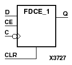
FDCE_1 is a single D-type flip-flop with data (D), clock enable (CE), asynchronous clear (CLR) inputs, and data output (Q). The asynchronous CLR input, when High, overrides all other inputs and sets the Q output Low. The data on the D input is loaded into the flip-flop when CLR is Low and CE is High on the High-to-Low clock (C) transition. When CE is Low, the clock transitions are ignored.
The flip-flop is asynchronously cleared, output Low, when power is applied. FPGAs simulate power-on when global reset (GR) or global set/reset (GSR) is active. GR for XC3000 is active-Low. GR for XC5200 and GSR (XC4000, Spartans, Virtex) default to active-High but can be inverted by adding an inverter in front of the GR/GSR input of the STARTUP or STARTUP_VIRTEX symbol.
| Inputs | Outputs | |||
|---|---|---|---|---|
| CLR | CE | D | C | Q |
| 1 | X | X | X | 0 |
| 0 | 0 | X | No Chg | |
| 0 | 1 | 1 | 1 | |
| 0 | 1 | 0 | 0 | |
Figure 5.13 FDCE_1 Implementation XC3000, XC4000, XC5200, Spartans |