| XC3000 | XC4000E | XC4000X | XC5200 | XC9000 | Spartan | SpartanXL | Virtex |
|---|---|---|---|---|---|---|---|
| Primitive | N/A | N/A | N/A | N/A | N/A | N/A | N/A |

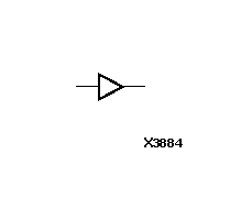
GCLK, the global clock buffer, distributes high fan-out clock signals. One GCLK buffer on each device provides direct access to every Configurable Logic Block (CLB) and Input Output Block (IOB) clock pin. If it is not used in a design, its routing resources are not used for any signals. Therefore, the GCLK should always be used for the highest fan-out clock net in the design. The GCLK input (I) can come from one of the following sources.
The output of the GCLK buffer can drive all the clock inputs on the chip, but it cannot drive non-clock inputs. For a negative-edge clock, insert an INV (inverter) element between the GCLK output and the clock input. This inversion is performed inside the CLB, or in the case of IOB clock pins, on the IOB clock line (which controls the clock sense for the IOBs on an entire edge of the chip).