| XC3000 | XC4000E | XC4000X | XC5200 | XC9000 | Spartan | SpartanXL | Virtex |
|---|---|---|---|---|---|---|---|
| N/A | N/A | N/A | N/A | N/A | N/A | N/A | Primitive |


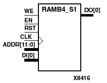
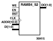
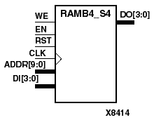
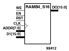
RAMB4_S1, RAMB4_S2, RAMB4_S4, RAMB4_S8, and RAMB4_S16 are dedicated random access memory blocks with synchronous write capability. They provide the capability for fast, discrete, large blocks of RAM in each Virtex device.The RAMB4_Sn cell configurations are listed in the following table.
| Component | Depth | Width | Address Bus | Data Bus |
|---|---|---|---|---|
| RAMB4_S1 | 4096 | 1 | (11:0) | (0:0) |
| RAMB4_S2 | 2048 | 2 | (10:0) | (1:0) |
| RAMB4_S4 | 1024 | 4 | (9:0) | (3:0) |
| RAMB4_S8 | 512 | 8 | (8:0) | (7:0) |
| RAMB4_S16 | 256 | 16 | (7:0) | (15:0) |
The enable (EN) pin controls read, write, and reset. When EN is Low, no data is written and the output (DO) retains the last state. When EN is High and reset (RST) is High, DO is cleared during the Low-to-High clock (CLK) transition; if write enable (WE) is High, the memory contents reflect the data at DI. When EN is High and WE is Low, the data stored in the RAM address (ADDR) is read during the Low-to-High clock transition. When EN and WE are High, the data on the data input (DI) is loaded into the word selected by the write address (ADDR) during the Low-to-High clock transition and the data output (DO) reflects the selected (addressed) word.
The above description assumes an active High EN, WE, RST, and CLK. However, the active level can be changed by placing an inverter on the port. Any inverter placed on a RAMB4 port is absorbed into the block and does not use a CLB resource.
RAMB4_Sn's may be initialized during configuration. See the “Specifying Initial Contents of a Block RAM” section below.
Block RAM output registers are asynchronously cleared, output Low, when power is applied. The initial contents of the block RAM are not altered. Virtex simulates power-on when global set/reset (GSR) is active. GSR defaults to active-High but can be inverted by adding an inverter in front of the GSR input of the STARTUP_VIRTEX symbol.
Mode selection is shown in the following truth table.
| Inputs | Outputs | ||||||
|---|---|---|---|---|---|---|---|
| EN | RST | WE | CLK | ADDR | DI | DO | RAM Contents |
| 0 | X | X | X | X | X | No Chg | No Chg |
| 1 | 1 | 0 | X | X | 0 | No Chg | |
| 1 | 1 | 1 | addr | data | 0 | RAM(addr) <=data | |
| 1 | 0 | 0 | addr | X | RAM(addr) | No Chg | |
| 1 | 0 | 1 | addr | data | data | RAM(addr) <=data | |
| addr=RAM address RAM(addr)=RAM contents at address ADDR data=RAM input data | |||||||
You can use the INIT_0x attributes to specify an initial value during device configuration. The initialization of each RAMB4_Sn is set by 16 initialization attributes (INIT_00 through INIT_0F) of 64 hex values for a total of 4096 bits. See the “INIT_0x” section of the “Attributes, Constraints, and Carry Logic” chapter for more information on these attributes.
If any INIT_0x attribute is not specified, it is configured as zeros. Partial initialization strings are padded with zeros to the left.