HDL Designs with Black Box Instantiation
LogiBLOXs, schematics (EDIF file), ABEL modules, and XNF files can be instantiated in the VHDL and Verilog code using the “black box instantiation” method.
The Files tab in the Hierarchy Browser does not display the black box module name under the HDL file(s) in which it is instantiated.
This section describes how to create HDL designs that include black box instantiation in Foundation 1.5.
LogiBLOX RAM Module in a VHDL or Verilog Design
LogiBLOX modules may be generated in Foundation and then instantiated in the VHDL or Verilog code. This flow may be used for any LogiBLOX component, but it is especially useful for memory components such as RAM. Never describe RAM behaviorally in the HDL code, because combinatorial feedback paths will be inferred.
The module being instantiated must be located in the HDL project directory (that is, the directory where the top-level HDL file resides).
LogiBLOX provides a template tool for generating the VHDL or Verilog component declaration statement.
VHDL Instantiation
This section explains how to instantiate a LogiBLOX module into a VHDL design using Foundation 1.5. The example described below creates a RAM48X4S using LogiBLOX.
- Access the LogiBLOX Module Selector window using one of the following methods. Its operation is the same regardless of where it is invoked.
- From the Project Manger, select Tools
 Design Entry
  LogiBLOX module generator
- From the HDL Editor, select Synthesis
 LogiBLOX
- From Schematic Capture, select Options
 LogiBLOX
- Click Setup on the LogiBLOX Module Selector screen. (The first time LogiBLOX is invoked, the Setup screen appears automatically.)
- In the Setup window, enter the following items.
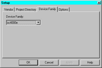
- Under the Device Family tab, use the pulldown list to select the target device family (XC4000E, for example).

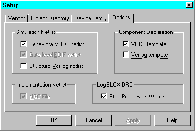
- Under the Options tab, select the Simulation Netlist and Component Declaration template.To instantiate the LogiBLOX module in VHDL code, select VHDL template in the Component Declaration area and Behavioral VHDL netlist in the Simulation Netlist area, as shown below. Click OK.

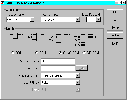
- In the LogiBLOX Module Selector window, define the type of LogiBLOX module and its attributes. The Module Name specified here is used as the name of the instantiation in the VHDL code.

- When you click OK, the LogiBLOX module is created automatically and added to the project library.
The LogiBLOX module is a collection of several files including those listed below. The files are located in your Xilinx project directory for the current project.
| component_name.ngc
| Netlist used during the Translate phase of Implementation
|
| component_name.vhi
| Instantiation template used to add a LogiBLOX module into your VHDL source code
|
| component_name.vhd
| VHDL file used for functional simulation
|
| component_name.mod
| Configuration information for the module
|
| logiblox.ini
| LogiBLOX configuration for the project
|
The component name is the name given to the LogiBLOX module in the GUI. The port names are the names provided in the .vhi file.
- In the HDL Editor, open the LogiBLOX-created .vhi file (memory.vhi) located under the current project. The .vhi file for the memory component created in the previous steps is shown below.
-----------------------------------------------
-- LogiBLOX SYNC_RAM Module "memory"
-- Created by LogiBLOX version M1.5.18
--    on Tue Jun 23 16:46:04 1998
-- Attributes
--    MODTYPE = SYNC_RAM
--    BUS_WIDTH = 4
--    DEPTH = 48
--    STYLE = MAX_SPEED
--    USE_RPM = FALSE
-----------------------------------------------
-----------------------------------------------
-- Component Declaration
-----------------------------------------------
component memory
PORT(
A: IN std_logic_vector(5 DOWNTO 0);
DO: OUT std_logic_vector(3 DOWNTO 0);
DI: IN std_logic_vector(3 DOWNTO 0);
WR_EN: IN std_logic;
WR_CLK: IN std_logic);
end component;
-----------------------------------------------
-- Component Instantiation
-----------------------------------------------
instance_name : memory port map
(A => ,
DO => ,
DI => ,
WR_EN => ,
WR_CLK => );
- Open a second session of the HDL Editor. In the second HDL Editor window, open the VHDL file in which the LogiBLOX component is to be instantiated. Cut and paste the Component Declaration from the LogiBLOX component's .vhi file to your project's VHDL code, placing it after the architecture statement in the VHDL code.
Cut and past the Component Instantiation from the LogiBLOX component's .vhi file to your VHDL design code after the “begin” line. Give the inserted code an instance name. Edit the code to connect the signals in the design to the ports of the LogiBLOX module.
The VHDL design code with the LogiBLOX instantiation for the component named memory is shown below. For each .ngc file from LogiBLOX, you may have one or more VHDL files with the .ngc file instantiated. In this example, there is only one black box instantiation of memory, but multiple calls to the same module may be done.
library IEEE;
   use IEEE.std_logic_1164.all;
   use IEEE.std_logic_arith.all;
   entity top is
   port (          D: in STD_LOGIC; CE: in STD_LOGIC;
                 CLK: in STD_LOGIC; Q: out STD_LOGIC;
                Atop: in STD_LOGIC_VECTOR (5 downto 0);
               DOtop: out STD_LOGIC_VECTOR (3 downto 0);
               DItop: in STD_LOGIC_VECTOR (3 downto 0);
            WR_ENtop: in STD_LOGIC;
           WR_CLKtop: in STD_LOGIC);
   end top;
   architecture inside of top is
   component userff
   port (    D: in STD_LOGIC; CE: in STD_LOGIC;
           CLK: in STD_LOGIC; Q:  out STD_LOGIC);
   end component;
   component memory
   port (    A:  in STD_LOGIC_VECTOR (5 downto 0);
             DI:  in STD_LOGIC_VECTOR (3 downto 0);
             WR_EN:  in STD_LOGIC;
             WR_CLK:   in STD_LOGIC;
             DO:  out STD_LOGIC_VECTOR (3 downto 0));
   end component;
   begin
   UO:userff port map (D=>D, CE=>CE, CLK=>CLK, Q=>Q);
   U1:memory port map(A=>Atop,DI=>DItop,WR_EN=>WR_ENtop,
                  WR_CLK=>WR_CLKtop, DO=>DOtop);
   end inside;
- Check the syntax of the VHDL design code by selecting Synthesis
 Check Syntax in the HDL Editor. Correct any errors. Then save the design and close the HDL Editor.
- The design with the instantiated LogiBLOX module can then be synthesized (click the Synthesis button on the Flow tab).
NOTEWhen the design is synthesized, a warning is generated that the LogiBLOX module is unexpanded. Modules instantiated as black boxes are not elaborated and optimized. The warning message is just reflecting the black box instantiation.
|
- To complete the design, refer to the “Synthesizing the Design”through the “Programming the Device” sections under the “All-HDL Designs” section.
NOTEThe instantiated module must be in the same directory as the HDL code in which it is instantiated.
|
Verilog Instantiation
This section explains how to instantiate a LogiBLOX module into a Verilog design using Foundation 1.5. The example described below creates a RAM48X4S using LogiBLOX.
- Access the LogiBLOX Module Selector window using one of the following methods. Its operation is the same regardless of where it is invoked.
- From the Project Manger, select Tools
 Design Entry
  LogiBLOX module generator.
- From the HDL Editor, select Synthesis
 LogiBLOX.
- From Schematic Capture, select Options
 LogiBLOX.
- Click Setup on the LogiBLOX Module Selector screen. (The first time LogiBLOX is invoked, the Setup screen appears automatically.)
- In the Setup window, enter the following items.
- Under the Device Family tab, use the pulldown list to select the target device family (XC4000E, for example).

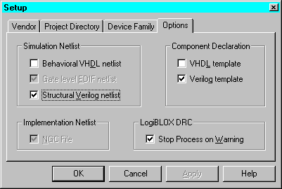
- Under the Options tab, select Verilog template in the Component Declaration area and select Structural Verilog netlist in the Simulation Netlist area, as shown below. Click OK.

- In the LogiBLOX Module Selector window, define the type of LogiBLOX module and its attributes. The Module Name specified here is used as the name of the instantiation in the Verilog code.

- When you click OK, the LogiBLOX module is created automatically and added to the project library.
The LogiBLOX module is a collection of several files including those listed below. The files are located in your Xilinx project directory for the current project.
| component_name.ngc
| Netlist used during the Translate phase of Implementation
|
| component_name.vei
| Instantiation template used to add LogiBLOX module into your Verilog source code
|
| component_name.v
| Verilog file used for functional simulation
|
| component_name.mod
| Configuration information for the module
|
| logiblox.ini
| LogiBLOX configuration for the project
|
The component name is the name given to the LogiBLOX module in the GUI. The port names are the names provided in the .vei file.
- In the HDL Editor, open the LogiBLOX- created .vei file (memory.vei) located under the current project. The .vei file for the memory component created in the previous steps is shown below.
//---------------------------------------------------
// LogiBLOX SYNC_RAM Module "memory"
// Created by LogiBLOX version M1.5.18
//    on Wed Jun 24 10:40:25 1998
// Attributes
//    MODTYPE = SYNC_RAM
//    BUS_WIDTH = 4
//    DEPTH = 48
//    STYLE = MAX_SPEED
//    USE_RPM = FALSE
//---------------------------------------------------
memory instance_name
( .A(),
  .DO(),
  .DI(),
  .WR_EN(),
  .WR_CLK());
module memory(A, DO, DI, WR_EN, WR_CLK);
input [5:0] A;<
output [3:0] DO;
input [3:0] DI;
input WR_EN;
input WR_CLK;
endmodule
- Open a second session of the HDL Editor. In the second HDL Editor window, open the Verilog design file in which the LogiBLOX component is to be instantiated.
Cut and paste the module declaration from the LogiBLOX component's .vei file into the Verilog design code, placing it after the “endmodule” line within the architecture section or the Verilog design code.
Cut and paste the component instantiation from the .vei file into the design code. Give the added code an instance name and edit it to connect the ports to the signals.
The Verilog design code with the LogiBLOX instantiation for the component named memory is shown below. For each .ngc file from LogiBLOX, you may have one or more VHDL files with the .ngc file instantiated. In this example, there is only one black box instantiation of memory, but multiple calls to the same module may be done.
module top (D,CE,CLK,Q,
               Atop, DOtop, DItop, WR_ENtop, WR_CLKtop);
   input D;
   input CE;
   input CLK;
   output Q;
   input  [5:0] Atop;
   output  [3:0] DOtop;
   input  [3:0] DItop;
   input WR_ENtop;
   input WR_CLKtop;
   userff U0  (.D(D),.CE(CE),.CLK(CLK),.Q(Q));
   memory U1  (  .A(Atop),
                 .DO (DOtop),
              .DI (DItop),
                 .WR_EN (WR_ENtop),
                 .WR_CLK (WR_CLKtop));
   endmodule
NOTEAn alternate method is to place the module declaration from the .vei file into a new, empty Verilog file (MRMORY.V) and add the new file (shown below) to the project.
| //---------------------------------------------------
// LogiBLOX SYNC_RAM Module "memory"
// Created by LogiBLOX version M1.5.18
// on Wed Jun 24 10:40:25 1998
// Attributes
// MODTYPE = SYNC_RAM
// BUS_WIDTH = 4
// DEPTH = 48
// STYLE = MAX_SPEED
// USE_RPM = FALSE
//---------------------------------------------------
module MRMORY (A, DO, DI, WR_EN, WR_CLK);
input [5:0] A;
output [3:0] DO;
input [3:0] DI;
input WR_EN;
input WR_CLK;
endmodule
- Check the syntax of the Verilog design code by selecting Synthesis
 Check Syntax in the HDL Editor. Correct any errors and then save the design and close the HDL Editor.
- The design with the instantiated LogiBLOX module can then be synthesized (click the Synthesis button on the Flow tab).
NOTEWhen the design is synthesized, a warning is generated that the LogiBLOX module is unexpanded. Modules instantiated as black boxes are not elaborated and optimized. The warning message is just reflecting the black box instantiation.
|
- To complete the design, refer to the “Synthesizing the Design” section through the “Programming the Device” section under the “All-HDL Designs” section in this chapter.
NOTEThe instantiated module must be in the same directory as the HDL code in which it is instantiated.
|
XNF file in a VHDL or Verilog Design
This section explains how to instantiate an XNF file as a black box in a VHDL or Verilog design. This procedure only works for Xilinx Unified Library XNF files.
- Open the XNF file with a text editor. Search for the string LCANET.
The LCANET line must be either LCANET, 5 or LCANET, 6. If the search for LCANET turns up an LCANET, 4 or earlier, this XNF file cannot be used in the F1.5 (or M1) flows. Please see the M1 Conversion Guide on the Xilinx website for details on handling pre-Unified XNF files (LCANET, 4 or earlier).
The name of the XNF file must be the name of the "component" instantiation in the VHDL code or the name of the "module" instantiation in the Verilog code.
- To attach the XNF module in the VHDL or Verilog code, use the nets named in the PIN records and/or SIG records in the XNF file as the port names of the component instantiation. The following is an example XNF file with PIN and SIG records.
SYM, current_state_reg<4>, DFF, LIBVER=2.0.0
PIN, D, I, next_state<4>, ,
PIN, C, I, N10, ,
PIN, Q, O, current_state<4>, ,
END
SIG, current_state<4>
SIG, CLK, I, ,
SIG, DATA, I, ,
SIG, SYNCFLG, O, ,
To reference buses in the instantiation of XNF modules, the nets named in PIN records and/or SIG records must be of the form.
netname<number>
This designation allows the bus to be referenced in the VHDL component as a vector data type.
- Using the filename of the XNF file as the name of the component and the name of nets in the XNF file as port names, instantiate the XNF file in the VHDL or Verilog code.
- The design with the instantiated XNF black box can then be synthesized (click the Synthesis button on the Flow tab).
NOTEWhen the design is synthesized, a warning is generated that the XNF module is unexpanded. Modules instantiated as black boxes are not elaborated and optimized. The warning message is just reflecting the black box instantiation. Expansion of the XNF module takes place during the Translation stage of the Implementation phase.
|
- To complete the design, refer to the “Synthesizing the Design”through the “Programming the Device” sections under the “All-HDL Designs” section.
NOTEThe instantiated module must be in the same directory as the HDL code in which it is instantiated.
|
Schematic (EDIF file) in a VHDL or Verilog Design
You can create schematics in Foundation which can then be instantiated as a black box in a VHDL or Verilog file. The schematic must have hierarchy connectors at each of the ports in order for the connection between the HDL top-level design and the lower-level schematic module to be realized.
The following procedure shows how to instantiate a purely schematic design into an HDL Flow project.
- Open Schematic Capture by clicking the Schematic Capture icon in the Design Entry box on the Project Manager's Flow tab.

- Create the schematic in Schematic Capture. The schematic, as in the following example, must not have I/O library components like IBUF, OBUF, OBUFT. In the schematic, use hierarchy connectors in place of I/O components. The name of the hierarchy connectors will be the name of the pins for the instantiation in the HDL code. The schematic can contain hierarchy.

- Save the schematic by selecting File
 Save As and choose a name for the module. Save the file to your Foundation project directory, but do not add the schematic to the project.
- Select Options
 Create Netlist from Current Sheet.
- Select Options
 Export Netlist. Select the newly created netlist and make sure that the file is exported to the .edn format.
This step creates an EDIF file in the Foundation Project Manager. The EDIF file will have the extension .edn, and the project name will be the name of the EDIF file.
- Instantiate the Foundation schematic.
- For VHDL, instantiate the Foundation schematic, using the schematic module name as the instantiated module name and the name of the hierarchy connectors as the names of the pins. In this example, the EDIF file was created in a project called test1.
library IEEE;
use IEEE.std_logic_1164.all
use IEEE.std_logic_unsgned.all;
entity test is
port ( FIRST: in STD_LOGIC;
      SECOND: in STD_LOGIC;
       THIRD: in STD_LOGIC);
end test;
architecture inside of test is
component test1
port (A:in STD_LOGIC;B:in STD_LOGIC;C:out STD_LOGIC);
end component;
begin
U1: test1 port map(A=>FIRST,B=>SECOND,C=>THIRD0;
end inside;
- For Verilog, instantiate the Foundation schematic, using the schematic module name as the instantiated module name and the name of the hierarchy connectors as the name of the pins. In the following example, the EDIF file was created in a project called test1.
module test (FIRST,SECOND,THIRD);
input FIRST;
input SECOND;
output THIRD;
test1 U1 (.A(FIRST),.B(SEDOND),.C(THIRD));
endmodule
- The HDL design with the instantiated EDIF file can then be synthesized (click the Synthesis button on the Flow tab).
NOTEWhen the design is synthesized, a warning is generated that the EDIF schematic module is unexpanded. Modules instantiated as black boxes are not elaborated and optimized. The warning message is just reflecting the black box instantiation. Expansion of the EDIF module takes place during the Translation stage of the Implementation phase.
|
- To complete the design, refer to the “Synthesizing the Design”through the “Programming the Device” sections under the “All-HDL Designs” section.
NOTEThe instantiated file must be in the same directory as the HDL code in which it is instantiated.
| 
