| XC3000 | XC4000E | XC4000X | XC5200 | XC9000 | Spartan | SpartanXL | Virtex |
|---|---|---|---|---|---|---|---|
| N/A | Macro | Macro | Macro | N/A | Macro | Macro | Macro |


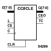
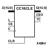
CC8CLE and CC16CLE are, respectively, 8- and 16-bit (stage), synchronously loadable, asynchronously clearable, cascadable binary counter. These counters are implemented using carry logic with relative location constraints to ensure efficient placement of logic.
The asynchronous clear (CLR) is the highest priority input. When CLR is High, all other inputs are ignored; the Q outputs, terminal count (TC), and clock enable out (CEO) go to logic level zero, independent of clock transitions. The data on the D inputs is loaded into the counter when the load enable input (L) is High during the Low-to-High clock (C) transition, independent of the state of clock enable (CE). The Q outputs increment when CE is High during the Low-to-High clock transition. The counter ignores clock transitions when CE is Low. The TC output is High when all Q outputs are High.
Larger counters are created by connecting the count enable out (CEO) output of the first stage to the CE input of the next stage and connecting the C, L, and CLR inputs in parallel. CEO is active (High) when TC and CE are High. The maximum length of the counter is determined by the accumulated CE-to-TC propagation delays versus the clock period. The clock period must be greater than n(tCE-TC), where n is the number of stages and the time tCE-TC is the CE-to-TC propagation delay of each stage. When cascading counters, use the CEO output if the counter uses the CE input; use the TC output if it does not.
The counter is asynchronously cleared, with Low output, when power is applied. FPGAs simulate power-on when global reset (GR) or global set/reset (GSR) is active. GR for XC5200 and GSR (XC4000, Spartans, Virtex) default to active-High but can be inverted by adding an inverter in front of the GR/GSR input of the STARTUP or STARTUP_VIRTEX symbol.
| Inputs | Outputs | ||||||
|---|---|---|---|---|---|---|---|
| CLR | L | CE | C | Dz - D0 | Qz - Q0 | TC | CEO |
| 1 | X | X | X | X | 0 | 0 | 0 |
| 0 | 1 | X | Dn | dn | TC | CEO | |
| 0 | 0 | 0 | X | X | No Chg | No Chg | 0 |
| 0 | 0 | 1 | X | Inc | TC | CEO | |
| z = 7 for CC8CLE; z = 15 for CC16CLE dn = state of referenced input (Dn) one setup time prior to active clock transition TC = Qz•Q(z-1)•Q(z-2)•...•Q0 CEO = TC•CE | |||||||
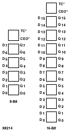
This is the CC8CLE (8-bit) and CC16CLE (16-bit) topology for XC4000 and Spartan series devices.

In the process of combining the logic that loads CEO and TC, the place and route software might map the logic that generates CEO and TC to different function generators. If this mapping occurs, the CEO and TC logic cannot be placed in the uppermost CLB as indicated in the illustration.
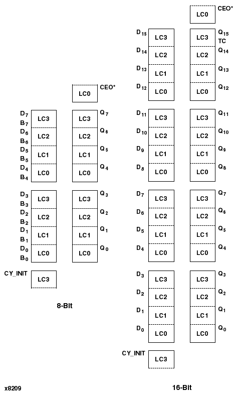
This is the CC8CLE (8-bit) and CC16CLE (16-bit) topology for XC5200 devices.

Figure 4.21 CC8CLE Implementation XC4000, Spartans |
Figure 4.22 CC8CLE Implementation XC5200 |
Figure 4.23 CC8CLE Implementation Virtex |