All-Schematic Designs
The following procedure describes how to create a top-level schematic design that contains schematics only, that is, there are no instantiated HDL or State Machine macros.
Creating the Schematic and Generating a Netlist
This section lists the basic steps for creating a schematic and generating a netlist from it.
- Open Schematic Capture by selecting the Schematic Capture icon from the Design Entry box on the Project Manager's Flow tab.

- Select Mode
 Symbols to add components to your new schematic. Select specific components from the SC Symbols window.
- Complete your schematic by placing additional components from the Symbol toolbox including I/O ports, nets, buses, labels, and attributes.
- Save your schematic by selecting File
 Save.
Save.
For more information about schematic designs, see the “Schematic Design Entry” chapter or in the Schematic Capture window, select Help  Schematic Editor Help Contents.
Performing Functional Simulation
- Open the Logic Simulator by clicking the Functional Simulation icon in the Simulation box on the Project Manager's Flow tab.

The design is automatically loaded into the simulator. The Waveform Viewer window displays on top of the Logic Simulator window.
- Add signals by selecting Signal
 Add Signals.
- From the Signals Selection portion of the Components Selection for Waveform Viewer window, select the signals that you want to see in the simulator.
- Use CTRL-click to select multiple signals. Make sure you add output signals as well as input signals.
- Click Add and then Close. The signals are added to the Waveform Viewer in the Logic Simulator screen.
- Select Signal
 Add Stimulators from the Logic Simulator menu. The Stimulator Selection window displays.
- In the Stimulator Selection window, create the waveform stimulus by attaching stimulus to the inputs. For more details on how to use the Stimulus Selection window, click the Help button.
- After the stimulus has been applied to all inputs, click the Simulation Step icon on the Logic Simulator toolbar to perform a simulation step. The length of the step can be changed in the Simulation Step Value pulldown menu to the right of the Simulation Step box. (If the Simulator window is not open, select View
 Main Toolbar.)

- Verify that the output waveform is correct. Click the Step button repeatedly to continue simulating.
- To save the stimulus for future viewing or reuse, select File
 Save Waveform. Enter a file name with a .tve extension in the File name box of the Save Waveform window. Click OK.
For more information about saving and loading test vectors, from the Logic Simulator window, select Help  Logic Simulator Help Contents. Then select Simulator Reference
  Working With Waveforms
  Saving and Loading Waveforms.
Implementing the Design
- Click the Implementation icon in the Implementation box on the Project Manager's Flow tab.

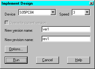
- The Implement Design dialog box appears.

By default, the Implementation targets the device that was previously selected when you created the project. If you want to retarget the design to a different device, use the Implement Design dialog box. If you want to retarget to a new device family, you must first do so in the Foundation Project Manager by selecting File  Project Type.
The first time you implement the design, a new version of the design is created and given the default version and revision name shown in the Implement Design dialog box. If you want, you can enter your own version or revision names.
On successive implementations of the design, a new revision is created for the current version and given the default revision name shown in the Implement Design dialog box. Or, you can select to overwrite the current revision.
If you want to implement a new version of the design (after the initial implementation), you must first create the new version by selecting Project  Create Version. This accesses the New Version dialog box. Click OK to accept the default name or enter a new name and click OK. Then implement the design.
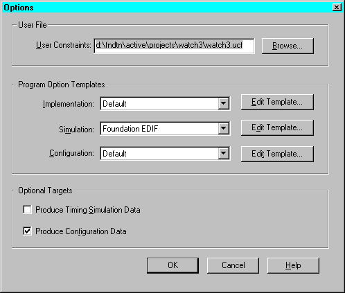
- In the Implement Design dialog box, select Options. The Options dialog box displays.

- Choose any desired implementation option. If you are planning on conducting a timing simulation, select the Produce Timing Simulation Data option.
- Click OK to return to the Implement Design dialog box.
- Click Run to implement your design. The Flow Engine displays the progress of the implementation.
When Implementation is complete, a dialog box appears indicating whether implementation was successful or not.
For more information on the Flow Engine, refer to the “Design Implementation” chapter or select Help Foundation Help Contents
 Flow Engine.
- Select the Reports tab on the Project Manager window to review your design reports (Implementation Report Files).
Verifying the Design
Performing a Static Timing Analysis (Optional)
- Click the Timing Analyzer icon in the Verification box on the Project Manager's Flow tab.

- Perform a static timing analysis on mapped or placed and routed designs for FPGAs.
For FPGAs, you can perform a post-MAP or post-place timing analysis to obtain rough timing information before routing delays are added. You can also perform a post-implementation timing analysis on CPLDs after a design has been implemented using the CPLD fitter.
For details on how to use the Timing Analyzer, select Help Foundation Help Contents
 Timing Analyzer.
Performing a Timing Simulation
- Open the Timing Simulator by clicking the Timing Simulation icon in the Verification box on the Project Managers's Flow tab. The implementation timing netlist will be loaded into the simulator.

- The Waveform Viewer window displays on top of the Logic Simulator window.
Refer to the “Performing Functional Simulation” section for instructions on simulating the design. (The operation of the simulator is the same for functional and timing simulation.)
- If you have already saved test vectors (for instance, in the functional simulation), you may load these vectors into the timing simulator by selecting File
 Load Waveform.
Programming the Device
- Click the Device Programming icon in the Programming box on the Project Manager's Flow tab.

- From the Select Program box, choose the Hardware Debugger, the PROM File Formatter, or the JTAG Programmer.
For CPLD designs, you must use the JTAG Programmer. For instructions, select Help  Foundation Help Contents
  Advanced Tools
  JTAG Programmer.
For FPGA designs, use the JTAG Programmer, Hardware Debugger, or PROM File Formatter. For instructions, select Help  Foundation Help Contents
  Advanced Tools and then select the desired tool.


![]() Schematic Editor Help Contents.
Schematic Editor Help Contents.


![]() Foundation Help Contents
Foundation Help Contents![]() Timing Analyzer.
Timing Analyzer.
